Fermi Level In Semiconductor : Fermi level in intrinsic semiconductor - T is the absolute temperature.
Fermi Level In Semiconductor : Fermi level in intrinsic semiconductor - T is the absolute temperature.. 1.1 0, indicating equal concentrations of electrons and holes. Kb is the boltzmann constant. So, it is detrimental, it is a major source of degradation in. That phenomenon is called the fermi level pinning and it takes away a very very important degree of freedom for engineering for semiconductor devices. In an extrinsic semiconductor, with the dopants fully ionized, there is an imbalance in the electron and hole concentration.
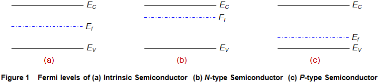
It doesn't matter how lightly or how heavily doped your semiconductor, your fermi level will always get stuck at that energy level. The fermi level lies between the valence band and conduction band because at absolute zero temperature the electrons are all in the lowest energy state. Fermi level lies in the midway between the valence band top and conduction band bottom of an intrinsic semiconductor, as shown in fig. I can understand that the distribution changes with the temperatures (it gets broader) but i don't understand why/how the fermi level changes. Of free electrons in conduction band.
Fermi Dirac Distribution Function | Electrical4U from www.electrical4u.com The fermi level lies between the valence band and conduction band because at absolute zero temperature the electrons are all in the lowest energy state. The fermi level is referred to as the electron chemical potential in other contexts. The fermi level plays an important role in the band theory of solids. However, for insulators/semiconductors, the fermi level can. I can understand that the distribution changes with the temperatures (it gets broader) but i don't understand why/how the fermi level changes. Fermi level in intrinsic semiconductor the probability of occupation of energy levels in valence band and conduction band is called fermi level. Of holes in valance band. Fermi level of extrinsic semiconductor extrinsic semiconductors are formed by adding suitable impurities to the intrinsic semiconductor.
The fermi level and band gap in a solid largely determine its electrical properties.
K.consequently, we see from this equation that the fermi level should typically lie very close to the middle of the energy gap in intrinsic semiconductors. Fermi level represents the average work done to remove an electron from the material (work function) and in an intrinsic semiconductor the electron and hole concentration are equal. In this case the fermi level is defined as the level in which the probability of occupation of electron at that energy is ½. Fermi level is a kind of measure of equilibrium electronic energy of a solid material. It is well estblished for metallic systems. The fermi level is the energy separating occupied states of the valence band from empty states of the conduction band at the absolute temperature t=0 kelvin. Of holes in valance band. The added impurity is very small, of the order of one atom. The semiconductor equations lecture 5.3: The correction term is small at room temperature since eg ~ 1 ev while kbt ~ 0.025 ev. Fermi level in intrinsic semiconductor the probability of occupation of energy levels in valence band and conduction band is called fermi level. • all energy level in one band is same energy. If you can bring the fermi level high enough, then part of the tail will go over to the conduction band.
Fermi level is a kind of measure of equilibrium electronic energy of a solid material. In this case the fermi level is defined as the level in which the probability of occupation of electron at that energy is ½. Whenever the system is at the fermi level, the population n is equal to 1/2. However, for insulators/semiconductors, the fermi level can. The fermi level is referred to as the electron chemical potential in other contexts.
What is Fermi-level pinning, and how could it affect the ... from qph.fs.quoracdn.net Kb is the boltzmann constant. The added impurity is very small, of the order of one atom. If you can bring the fermi level high enough, then part of the tail will go over to the conduction band. The correction term is small at room temperature since eg ~ 1 ev while kbt ~ 0.025 ev. The term fermi level is mainly used in discussing the solid state physics of electrons in semiconductors, and a precise usage of this term is necessary to describe band diagrams in devices comprising different materials with different levels of doping. Ec is the conduction band. It is well estblished for metallic systems. Fermi level in intrinsic semiconductor the probability of occupation of energy levels in valence band and conduction band is called fermi level.
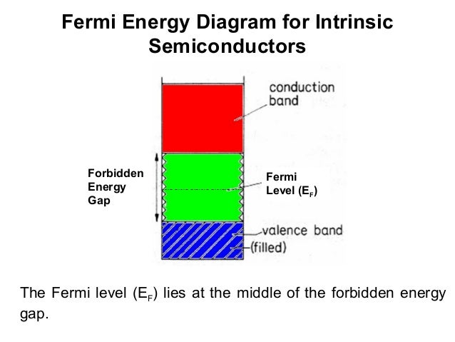
In semiconductors the position of the fermi level is within the band gap, approximately in the middle of the band gap.
Fermi level of extrinsic semiconductor extrinsic semiconductors are formed by adding suitable impurities to the intrinsic semiconductor. In a perfect semiconductor (in the absence of impurities/dopants), the fermi level lies close to the middle of the band gap 1. For si and ge, nc > nv and the correction term is negative while for gaas nc < nv and the correction term is positive. It is well estblished for metallic systems. At absolute zero temperature intrinsic semiconductor acts as perfect insulator. Whenever the system is at the fermi level, the population n is equal to 1/2. Due to lack of sufficient energy at 0 kelvin, the fermi level can be considered as the sea of fermions (or electrons) above which no electrons exist. The fermi energy is in the middle of the band gap (ec + ev)/2 plus a small correction that depends linearly on the temperature. The fermi level plays an important role in the band theory of solids. In an extrinsic semiconductor, with the dopants fully ionized, there is an imbalance in the electron and hole concentration. However, for insulators/semiconductors, the fermi level can. In metals, the fermi level lies in the hypothetical conduction band giving rise to free conduction electrons. Ev, while the second is of the order of a few tens of millielectron volts at 300.
The fermi level lies between the valence band and conduction band because at absolute zero temperature the electrons are all in the lowest energy state. However as the temperature increases free electrons and holes gets generated. For si and ge, nc > nv and the correction term is negative while for gaas nc < nv and the correction term is positive. Where the fermi energy is located (correct?). That phenomenon is called the fermi level pinning and it takes away a very very important degree of freedom for engineering for semiconductor devices.
semiconductor physics,unit 5 from image.slidesharecdn.com The fermi energy is in the middle of the band gap (ec + ev)/2 plus a small correction that depends linearly on the temperature. Due to lack of sufficient energy at 0 kelvin, the fermi level can be considered as the sea of fermions (or electrons) above which no electrons exist. The fermi level is the surface of fermi sea at absolute zero where no electrons will have enough energy to rise above the surface. Ec is the conduction band. In metals, the fermi level lies in the hypothetical conduction band giving rise to free conduction electrons. Fermi level is a kind of measure of equilibrium electronic energy of a solid material. For si and ge, nc > nv and the correction term is negative while for gaas nc < nv and the correction term is positive. The fermi level is referred to as the electron chemical potential in other contexts.
Fermi level is a kind of measure of equilibrium electronic energy of a solid material.
So, it is detrimental, it is a major source of degradation in. Fermi level is a kind of measure of equilibrium electronic energy of a solid material. Position of fermi level in intrinsic semiconductors • width of conduction band and valence band is small as compared to forbidden energy gap. The fermi level and band gap in a solid largely determine its electrical properties. Fermi level of extrinsic semiconductor extrinsic semiconductors are formed by adding suitable impurities to the intrinsic semiconductor. The correction term is small at room temperature since eg ~ 1 ev while kbt ~ 0.025 ev. Of electrons in conduction band are greater than no. Ohtani, in advances in inorganic chemistry, 2011 d fermi level. Fermi level lies in the midway between the valence band top and conduction band bottom of an intrinsic semiconductor, as shown in fig. For si and ge, nc > nv and the correction term is negative while for gaas nc < nv and the correction term is positive. Primer on semiconductors unit 5: Whenever the system is at the fermi level, the population n is equal to 1/2. Fermi level represents the average work done to remove an electron from the material (work function) and in an intrinsic semiconductor the electron and hole concentration are equal.
0 Response to "Fermi Level In Semiconductor : Fermi level in intrinsic semiconductor - T is the absolute temperature."

0 Response to "Fermi Level In Semiconductor : Fermi level in intrinsic semiconductor - T is the absolute temperature."
Post a Comment